Earlier this week Applied Materials Inc., the largest supplier of chipmaking equipment for smartphones and other cutting-edge computer technology, made waves in the industry when it announced the acquisition of the third-largest chipmaker, Tokyo Electron.
The deal, valued at $9.39 billion in stock and expected to close in mid 2014, would create a new tech giant valued at $29 billion that would control more than a quarter of the market in the rapidly evolving digital sector, which is shifting from personal computers to smaller, faster and more complex mobile devices.
The impact of the major deal is reverberating in Kalispell, where Applied Materials operates its Semitool Business Unit off West Reserve Drive.
The local facility plays a key role in the Applied Materials supply chain, developing components that are used within the massive company to create semiconductor and display technology that are then used by other companies to make the world’s most popular electronics.
Bill McClintock, the corporate vice president and general manager for the Semitool site, said significant upgrades are planned at the Kalispell facility, although they are not directly connected to the recent acquisition. More than $5 million worth of new lab equipment and other improvements are going to be installed in the Semitool facility early next year, McClintock said.
McClintock said the Semitool facility is already in the stages of changing a few opportunities within the local site, particularly by developing a wide array of equipment parts that can be used within the greater Applied Materials company.
“There’s great capacity in both manufacturing and machining in Kalispell,” he said. “A lot of times we need quick turns and high quality parts; Kalispell can do that for us.”
After the deal closes, Applied Materials shareholders will own about 68 percent of the new company. The companies expect to achieve $250 million in annualized run-rate operating synergies by the end of the first full fiscal year and $500 million in run-rate operating synergies realized in the third full fiscal year.
Based in Santa Clara, Calif., Applied Materials operates 86 facilities in 18 countries. The company’s net income dropped over the past two years amid the transforming semiconductor industry.
 |
|
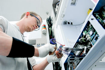
Lee Wirkus works on installing wires at the Semitool Business Unit of Applied Materials in Kalispell. – File photo by Lido Vizzutti/Flathead Beacon |
Mobile devices, which have replaced PCs as the most popular consumer technology, are driving a new phase of industry growth and introducing dramatic and fundamental technology changes in the way devices are made, which ties directly to Applied Materials’ efforts as the largest semiconductor developer.
By joining forces with Tokyo Electron, officials from Applied Materials say the combined organization will accelerate the existing strategic visions and lead to greater innovation.
“Today, we are launching a new company and taking a bold step forward for our industry,” Tetsuro Higashi, Chairman, president and CEO of Tokyo Electron, said in a statement. “Built on a foundation of people, technology and commitment, we are creating a truly global company that we believe will expand the value we deliver to our customers and be able to achieve new levels of financial performance.”